
Also known as a printed circuit board, PCB is used to join the electricity of the electric components with the use of signal traces and conductive pathways. These will run through processing from copper sheets, which have been layered to become non-conductive substrate.
Before ever placing the first component, you need to familiarize yourself with how to handle the PCB design grid to help you to be more productive as you place components, route traces, and join reference designators and other text. A specific PCB charged with electronic components known as PCB assembly or printed circuit board assembly. These are normally present in almost all the easiest electronic devices, which are commercially manufactured.
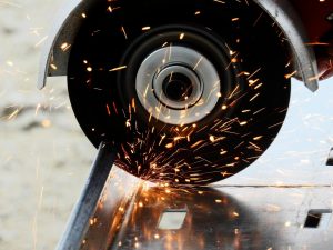
Once the PCB is finished, then electronic components can be connected to construct a printed circuit assembly. The edges of the elements are placed in surface-mount construction, and into the holes in the PCB. The electronic components are set on pads or lands on the exterior surfaces of the printed circuit board. The component elements are then automatically fixed to the PCB with a soft metal molten solder.
Construction Methods
There are different ways for connecting components to printed circuit boards, and the most very high capacity production is usually produced by machine placement and reflow ovens or bulk wave soldering. There are two classes of construction techniques used for the assembly.
1) Surface-Mount construction: Elements are set on pads or lands on the exterior of the printed circuit board
2) Through-Hole construction: Element is placed into the holes.
However, in both production techniques, the elements are still automatically electrically attached to the PCB with a heated metal solder.
Depending on the boards needed to be assembled will decide how the components are going to be soldered. If it is for high production capacity, then soldering components to the Printed Circuit Board is best done by machine placement. Machine placement is done with reflow oven or bulk wave soldering. Otherwise, if the production volume is for small quantity prototypes, joining by hand will work just fine in most instances.
Testing
One reason to apply both of the above methods is that surface mount procedure takes up less space and will go mostly unstressed, while the hole mounting can produce the required strength for any components which endures the physical stress. Once the PCB has been created or populated with the sought components, it can be tested in several different ways, and these may include:
Power off; analog signature analysis, power-off testing
Power on; check for functional test, if the PCB is doing what it is designed for
Power off; visual inspection & automated optical inspection
Power on; in-circuit test, physical measurements
PCB has a conformal coating that is applied by spraying or dipping once the components are done soldering. This coat will primarily prevent the leaking and corrosion of current or likely shorting because of compression. PCB assembly is static sensitive, whereby; it should be placed inside antistatic bags while it is being transported. Inappropriate methods in handling could transmit static charges through the board and may damage the components.
A PCB is a printed circuit board. PCBs are a part of our everyday lives; wrist-watches, calculators, cellphones, computers, and every electrical component we interact with daily. The most common shape for PCB is a rectangle. Many individuals also prefer to have the corners rounded, as this reduces the likelihood of edge-cracking. With the help of a PCB design grid, the shapes will highly depend on what your mechanical requirements are and where you are going to place the board (the final box where the product is set).